What is IP design internship? Ever visited Pizza Hut?
IP (intellectual property) as the name suggests, is a property which is a result of creativity. Ever tasted Yummy Pizzas from Pizza Hut, which was […]
A dream and a mission statement that was framed 10 years back by VSD and efabless (or let us say, e-fabulous) has now taken a […]
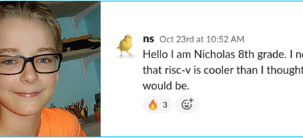
It was also a real testament to Nicholas’s thirst for knowledge and the outside-the-box thinking of his home-schooling parents, Rasa and Mike. Having a 13-year-old of my own, I was particularly impressed by Nicholas’s willingness to put himself out there, asking questions and joining Zoom calls (not to mention his familiarity with Linux). I’ve since learned that Nicholas has been awarded in spelling bees and math competitions and is an expert at solving the Rubik’s Cube. Somehow, I’m not surprised.
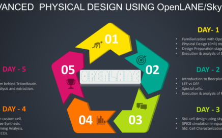
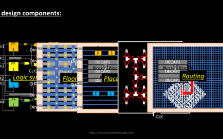
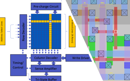
Know what Pentagon is? It is a plane figure which has 5-straight sides and 5-angles. For a perfect pentagon, it needs all its sides and angles to be the same, till the last decimal. Do you know what is the similarity between pentagon and our upcoming workshop “Advanced Physical Design workshop using OpenLANE/SKY130”? Look above image and you would guess it right. It is a perfect blend of topics where even a fresher can jump-start his/her career in chip design in just 5-days
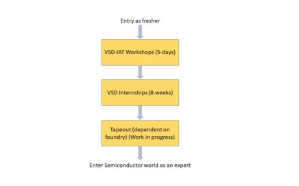
A great one – not only for VSD, but also for entire VSD community. The journey has just begun, in nutshell, below image shows a well-designed VLSI Skilling model (VSD Workshops + VSD-IP design Internship + Tapeout[working on it]), which is not just participants driven but also silicon proven. To summarize, given a problem statement, VSD Interns and participants, who have gone through this rigorous training and designing model will have much better ways to figure out solutions by themselves.
And that’s where VSD must play an especially important role to bring in latest and greatest VLSI skills to you, atleast in the field of open-source hardware. VSD owes a lot to VLSI community and hence has planned 3 exclusive cloud lab-based VLSI workshops on 3 important topics, with top 3 expert instructors from around globe, having more than 2 decades of experience – Tim Edwards, Steve Hoover, and Prof. Mohamed Shalan
Open-source EDA tool development with lab exercises using Sky130 pdk’s by Google/Skywater
RISC-V micro-architecture using transaction level – Verilog with lab exercises on Makerchip Platform
SoC and Physical Design using Automated RTL2GDS OpenLANE tool with lab exercises using demo design and Sky130 pdk’s.
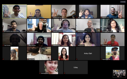
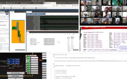
All the people whom you see in below image were a part of VSD 8-week Research IP design internship program, all interns are from colleges in India, and all of them built some cool analog IP’s from scratch. This internship program partially and unknowingly executes India’s ESDM vision and World’s open-source vision, all by college students, who passionately worked close to 14-15hours per day
VSD Research IP design 8-week internship were a series of stories about people and students reaching great heights, using available resources. Thanks to Pandemic, every VSD student from every corner of the world realized the power of open-source EDA for VLSI learning/trainings.
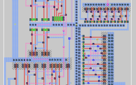
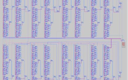
Ashutosh had joined our VSD Research IP design internship group 8-weeks back, along with 30 other interns. His journey on was from “I can’t, its too difficult” to “I did it”. Personally, only I know how hard it was for him when he saw an industry grade 10-bit DAC specifications on VSD IP website. We managed to achieve post-layout DNL of 3.5LSB and INL of 3.7LSB, which as per experience, is really tough for a fresher to achieve in a span of 8-weeks, but not impossible.
A full-fledged video lectures on step-by-step process to install OpenLANE EDA tool chain and Sky130 PDK open-process on your own laptop, from scratch. There is a dependency on vsdflow, though for fresh users and with Windows or fresh Unix machines. To do something like this, it needs a clear focus on end vision, with very good VLSI fundamentals, which demands hours of efforts every day