Foundry IP’s vs Macros – 10years to solve this query

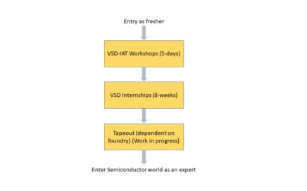
A great one – not only for VSD, but also for entire VSD community. The journey has just begun, in nutshell, below image shows a well-designed VLSI Skilling model (VSD Workshops + VSD-IP design Internship + Tapeout[working on it]), which is not just participants driven but also silicon proven. To summarize, given a problem statement, VSD Interns and participants, who have gone through this rigorous training and designing model will have much better ways to figure out solutions by themselves.
Continue reading

7th mile-stone in open-source analog IP design – 10-bit DAC

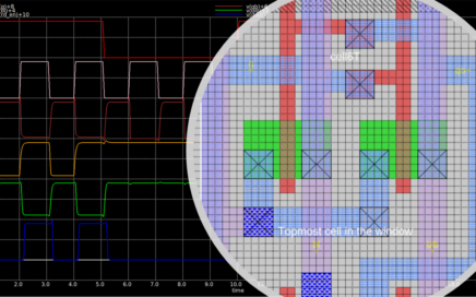
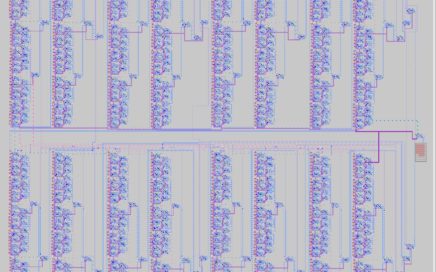
Ashutosh had joined our VSD Research IP design internship group 8-weeks back, along with 30 other interns. His journey on was from “I can’t, its too difficult” to “I did it”. Personally, only I know how hard it was for him when he saw an industry grade 10-bit DAC specifications on VSD IP website. We managed to achieve post-layout DNL of 3.5LSB and INL of 3.7LSB, which as per experience, is really tough for a fresher to achieve in a span of 8-weeks, but not impossible.

Continue reading

6th mile-stone in field of open-source – FREE VLSI tool installation course

A full-fledged video lectures on step-by-step process to install OpenLANE EDA tool chain and Sky130 PDK open-process on your own laptop, from scratch. There is a dependency on vsdflow, though for fresh users and with Windows or fresh Unix machines. To do something like this, it needs a clear focus on end vision, with very good VLSI fundamentals, which demands hours of efforts every day

Continue reading

2nd mile-stone in field open-source (open-lane EDA + Google/Sky130)

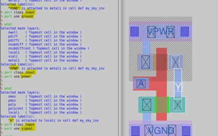
@Nickson joined our research project group under VSD Research internship program which runs for 8-weeks. He was supposed to develop flow for standard cell design and characterization using all open-source tools – magic/ngspice, then plug those standard cells into open-source PNR flow by open-lane, and benchmark RTL2GDS flow results. This needed a knowledge, not only of PNR, but device physics, custom layout, DRC/LVS and then (finally) Physical design/STA.

Continue reading