Hello

Now let me first be very clear – This blog is for freshers in static timing analysis domain. This topic had been very confusing even to me few years back as a fresher. May be it wasn’t documented in a way we would like to have it. I have tried my best (as usual) to clear this topic in detail in my course of STA-2, below is the link:
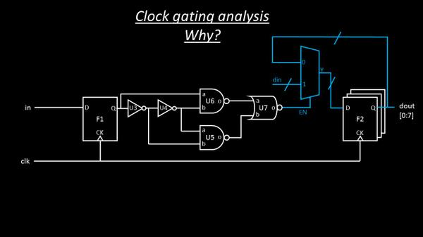
Let’s start with WHY we need it in the first place. Look into below image:

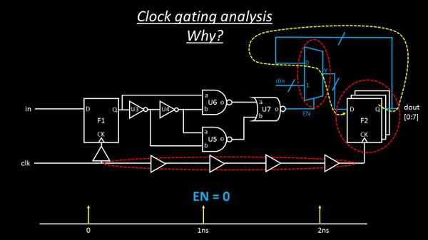
If the ‘EN’ pin of below mux is ‘1’, there’s a always a new data entering the register bank and eventually reaching dout[0:7]. But, when ‘EN’ pin is ‘0’, the registers and mux are doing nothing, but reloading the same data again and again at every clock cycle. This will result in immense power consumption every time same data in is loaded to data out and back to data in. There is no real value is wasting so much power for doing nothing. Would like to drain your mobile phone battery for no reason?
So here we need a mechanism to ‘gate’ the clock to the register bank, whenever there’s a situation like above (I have explained the scenario in even more detail in my STA-2 course)
Essential concepts and detailed interview guide.Your email address is 100% safe from spam!
Essential concepts and detailed interview guide.
Your email address is 100% safe from spam!
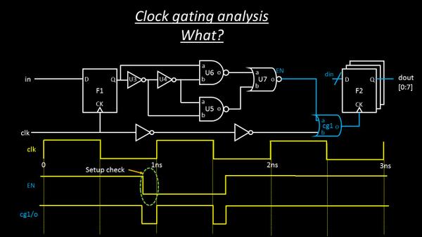
Now let’s look WHAT is clock gating technique. Look below image

Now here, I am putting an AND gate in capture clock path to register bank, that will open only when one of its input receives a ‘logic 1’ OR when ‘EN’ is high.
There’s a catch in above ‘EN’ signal. It can’t arrive anywhere in between the logic high or logic low level of clock signal, but, it needs to meet certain criteria, like if ‘EN’ goes high, it needs to go high before certain time of rising clock edge (resulting to setup-time check) and needs to remain high for the entire clock cycle ‘high’ (resulting in hold time check). This technique of using an ‘AND’ gate is referred to as ‘Active high’ clock gating technique. Can you figure out why? Because a high on ‘EN’ signal allows the clock cycle to hit register bank, thus allowing new data in to be loaded to data out.
Let’s find out HOW this technique helps: Well, you should have figured out till now. When your ‘EN’ is 0, the AND gate turns off, thus blocking clock to register bank, thereby retaining data out what it is, rather than reloading same data again and again (first image)
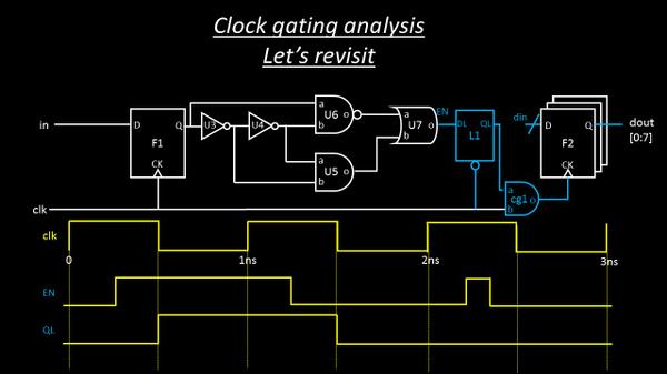
So how does ‘Active low’ clock gating looks like? Hmmmmm….look below image and you will be able to figure out, why below technique is called as ‘Active low’ clock gating

If still not able to figure out, no worries, I have explained this in detail in STA-2 course, for which below is the link.
And this is not it. There are complex setup timing and hold timing analysis needed to be done for the above clock gates. How do we do it? Wait n watch n explore in my STA-2 course
“All I wanted to do was to explore problems and areas where we didn’t have answers. In fact, where we didn’t even know the right questions to ask” – Donald Johnson
So get in and ask the right questions. I would be happy to help…
happy learning ….


