Partially and Unknowingly executed by VSD Interns!!
After yesterday’s VSD internship felicitation program, someone pointed out India’s National Policy on Electronics 2019 (NPE 2019) which envisages to position India as a global hub for ESDM (Electronics System Design & Manufacturing). This includes encouraging and driving capabilities in country for developing core components*
Someone also pointed out POSH (Posh Open Source Hardware) program by DARPA, which aims to develop and release a number of silicon-proven analog and digital IP blocks on an open-source platform to serve as foundation for rapid design of complex SoCs*
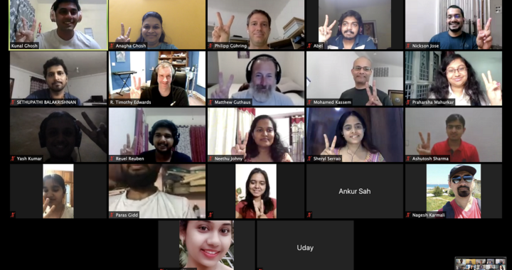
All the people whom you see in below image were a part of VSD 8-week Research IP design internship program, all interns are from colleges in India, and all of them built some cool analog IP’s from scratch. This internship program partially and unknowingly executes India’s ESDM vision and World’s open-source vision, all by college students, who passionately worked close to 14-15hours per day.
Suddenly it made us realize that all below interns, unknowingly, helped country and world take a huge leap in ESDM/open-source VLSI vision. You can observe and experiment their IP’s under below link.
https://www.vlsisystemdesign.com/ip/
Senior leaders from semi-conductor industry, VLSI freshers, VLSI recruiters, technical managers and everyone connected to VLSI – Let us (again) take a back-seat and congratulate all VSD interns for their immense contribution to our industry. And guess what – they are not done yet. This is just the beginning.
All VSD interns must go through a strict VSD-5SP (5-stage process) for 8-weeks. This process brings out smartest of everyone and a best version of themselves. VSD-5SP has a dependency on IP specifications and mentors.
Anyone senior VLSI member, looking to become VSD mentor in your free time, and contributing India’s and World’s vision – You are most welcome
Note – We still need Fab
*lines taken as is from respective program website

