Hello
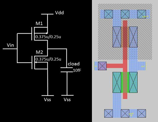
So can you identify what do the below images represent?

One is, of-course, the SPICE netlist of CMOS inverter, and the other one is the MAGIC layout of CMOS inverter. The image on the right side means a lot for the real world. It’s a way to connect designers of chip to manufacturers of a chip.
Let’s try to explore more on this topic. The image on the left hand side has got ‘zero’ dimension wires connecting transistors, power supply and ground. Whereas, image on the right side has ‘finite’ dimensions and ‘real’ contacts to connect each and every node. Do you know how does that matter to us? Look into the below waveforms
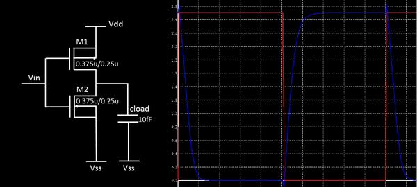
The above is the waveform from SPICE simulation of above inverter (‘zero’ size wire) and …….(sentence continued after below image)

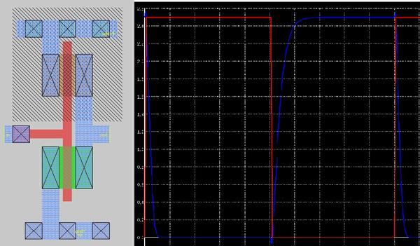
……..(sentence continued from above image) the above image is the waveform from SPICE simulation of inverter ‘extracted’ from above layout (MAGIC is a layout tool which has a feature to extract the SPICE netlist.. Stay tuned, and I will tell you how)
The waveforms of ‘zero’ wire size CMOS and ‘finite’ wire size CMOS looks so identical. This proves that the layout is functionally correct. But…..if you closely look into the delays of the inverter, its 58ps for ‘zero’ wire size CMOS and 68ps for ‘finite’ wire size CMOS. There is roughly ~10ps difference in the ‘drawn’ inverter and ‘fabricated’ inverter. That’s the key. Imagine a series of 100 such inverters on a chip. The cumulative delay difference in the inverter chain between ‘drawn’ and ‘fabricated’ will be approximately ~1000ps i.e. close to 1ns. That’s huge!! And hence, we need to understand, how ‘real’ is different from ‘drawn’
I am happy to announce that this will be the topic of my next course (not published yet) which will be called as “VLSI Academy – Design rules and custom layout”. This course will mainly focus on design rules needed for fabricating a design onto a chip, subckt design and an application design, namely SRAM.
‘New’ is always exciting….So stay excited, while I am getting ready to take you all to a world of layouts, and show you, how its so related to Static timing analysis
Happy Learning !!
