The Packaging Fundamentals of Design and Technology Workshop is designed to bridge the knowledge gap between traditional chip design and the cutting-edge world of packaging technologies. This program offers participants an in-depth understanding of modern packaging techniques, enabling them to make informed decisions when navigating the complexities of system-level integration.
Over the course of this workshop, you will gain hands-on insights into the evolution of packaging, advanced interconnect technologies, thermal simulations, assembly processes, and the critical decision-making processes involved in selecting the right packaging solutions.
We’ve tailored every aspect of the workshop to ensure an effective and enjoyable learning journey:
This workshop is designed for students, electronics and VLSI design engineers, packaging specialists, and professionals interested in understanding semiconductor packaging technologies.
A basic understanding of semiconductor design and fabrication is recommended. Familiarity with chip manufacturing processes is helpful but not mandatory.
Yes, participants will receive a certificate upon successful completion of the workshop.
The workshop includes practical training with industry-standard tools like ANSYS Icepak and AEDT (Ansys Electronics Desktop) for thermal simulation and package design.
The workshop blends both theoretical concepts and practical lab sessions to ensure comprehensive learning.
The workshop runs for 1 week and is conducted in an online format, with a combination of lectures and hands-on practical sessions.
This workshop equips you with industry-relevant knowledge, practical skills, and hands-on experience with leading simulation tools, enhancing your employability in semiconductor packaging, design, and system integration fields.
Yes, the workshop will provide opportunities to interact with experienced professionals and industry experts.
Meet Your Guides to the World of VLSI Design
Dr. Tarun Kumar Agarwal is an Assistant Professor at the Indian Institute of Technology Gandhinagar since April 2021. Previously, he was a Postdoctoral Researcher at ETH Zurich (2018–2021) and worked as a Component Design Engineer at Intel Technologies India Pvt. Ltd. (2010–2012).
His research interests include benchmarking beyond-CMOS materials, modeling advanced nanoscale devices, and material-device-circuit co-design for alternative computing paradigms. Tarun has published 13 journal articles in top-tier journals like IEEE Transactions on Electron Devices and Scientific Reports. He has also presented 12 papers at prestigious international conferences, including IEDM and ESSDERC, and holds 1 U.S. patent on bilayer graphene tunneling transistors.
With extensive experience in both academia and industry, he combines theoretical rigor with practical insights, equipping students to excel in advanced electronics and semiconductor technologies.
+ 18% GST
Next Cohort will start in
VSD, standing as a trailblazing Semiconductor EdTech company and a community-based Technology Aggregator, is revolutionizing the landscape of VLSI Design. With the belief that “Creativity is just connecting things”, VSD has mastered the art of linking the right resources with the community. This unique approach has sparked a significant transformation in the VLSI Design process.
Over the past decade, VSD has made remarkable strides in the open-source semiconductor domain. Our journey includes the development of comprehensive training content, empowering students to design silicon-grade IP/SoC. Notably, we’ve successfully guided these projects through the tapeout cycle via the Google open shuttle program. This achievement is a testament to our commitment to hands-on, practical education.
At VSD, our role extends beyond traditional education. While we didn’t invent EDA tools or design flows, we’ve made them accessible to a wider community. Our mentorship has been instrumental in the development of over 50+ Analog/Digital IPs and solutions. Impressively, 20+ of these have successfully transitioned from concept to Silicon – a clear indicator of our effective approach and the high quality of work produced under our guidance.
We pride ourselves on fostering a community-based revolution in the Semiconductor Industry. By democratizing access to advanced tools and knowledge, VSD is not just educating individuals; we are building a community of innovators poised to lead the next wave of advancements in the semiconductor sector. With VSD, the future of VLSI Design is not just being written; it’s being rewritten by a passionate and empowered community.
VSDSquadron was launched by Prof. V. Kamakoti, Director of IIT Madras
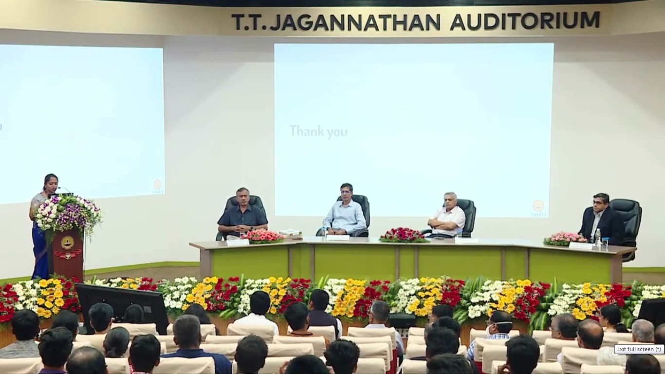
VSD Launches VSDSquadron In Collaboration With IIT Madras & DIR-V
Job Roles, Convergence With Embedded Systems, and Startups
VSD showcased at Semicon India 2023
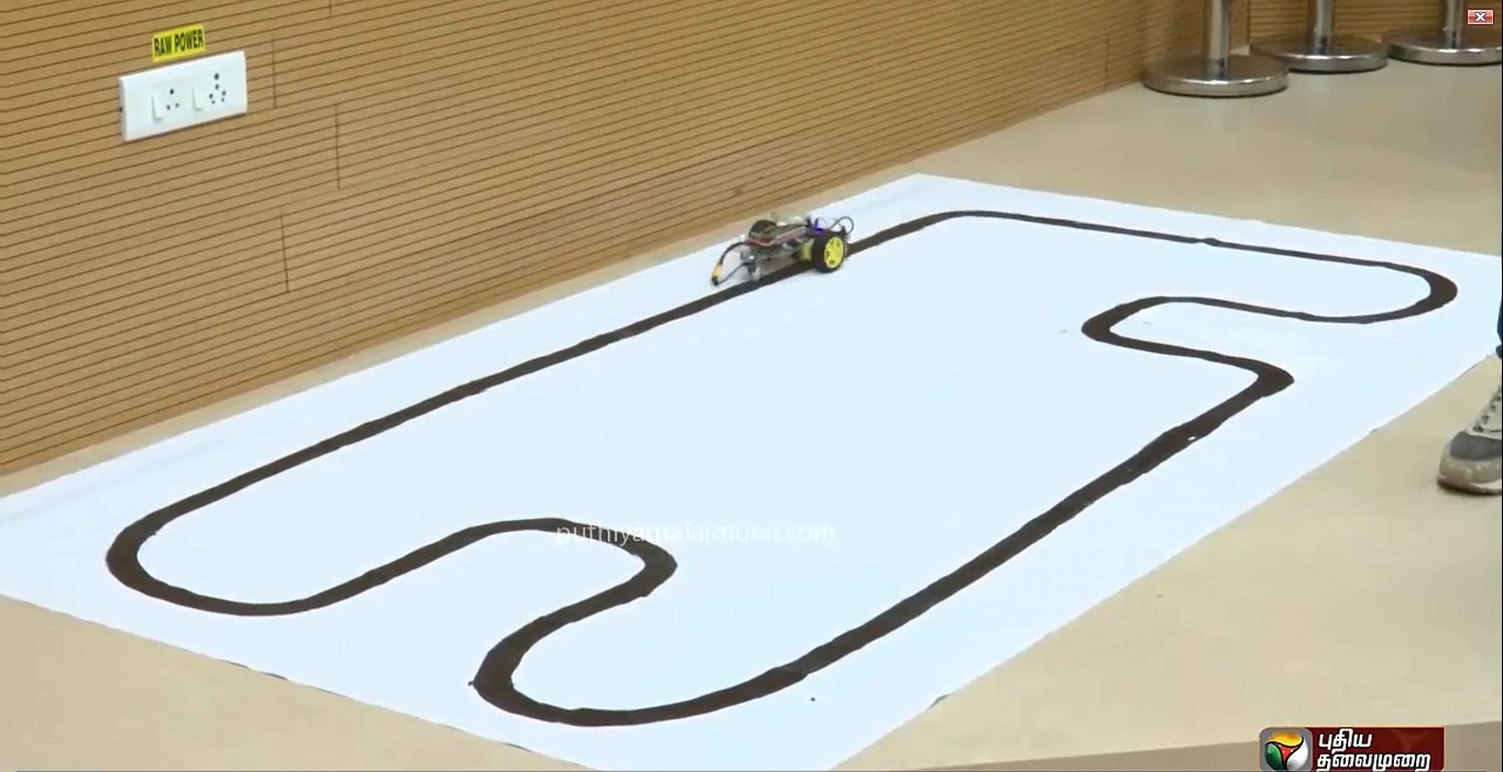
VSDSquadron Educational board on Tamil News channel
5 Day Workshop on VLSI Design Flow using RISCV and EDA Tools
Karnataka VLSI roadshow at Sahyadri College, Mangalore