This blog is regarding abstract submission for VSDOpen2018, which is the first online conference in VLSI, that covers all aspects of semiconductor technology with prime focus to build SoC using RISC-V CPU by illustrating exciting ways using (only) opensource EDA tools.
This conference has 6 symposium, out of which third symposium is to come up with innovative ways of Floorplanning to achieve best PPA. List of other symposium and session chair can be found in below link:
https://www.vlsisystemdesign.com/vsdopen2018-2/
This blog is about Symposium III – Floorplanning of digital IC’s for best area (abstract submission last date is 15th August, please see above link for details)
Couple of tips for submitting the best abstracts for Floorplanning will be take up any risc-v core (say picorv32 from Clifford Wolf or E31Core_Complex from SiFive) and synthesize digital blocks without pin hints to get the size of the digital block
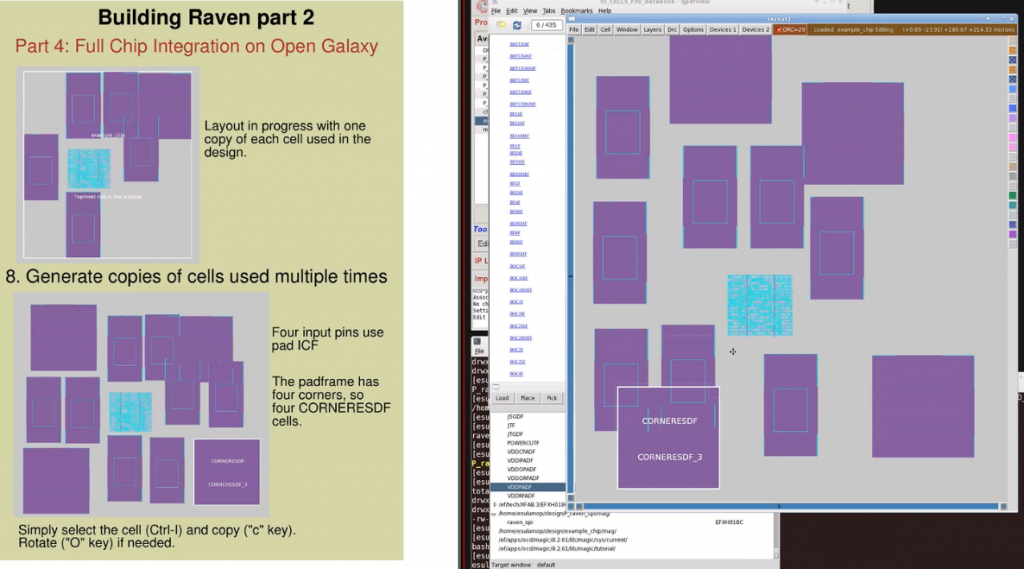
Next, place it inside the project and put pad-frame around it, which will help you to see what’s the size of the core compared to size of the pad-frame. Is my pad-frame dominating the whole chip? Do I need to use a different set of pads, from what’s available library? Let’s investigate the below small example of raven_spi from SoC physical design webinar which happened couple of weeks back

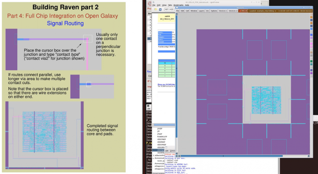
After that, make a quick layout with core and pads. If you have any another analog IP’s, add them. Then you figure out where your signals are supposed to go. If you have project specified already at the package level (like this is what your package is going to look like, this is where your pins are), you have your pin-constraints, you need to stick to that. If you don’t have that constraints, then you are free to decide the locations of your pins. The below is how core and pad placed chip will look like

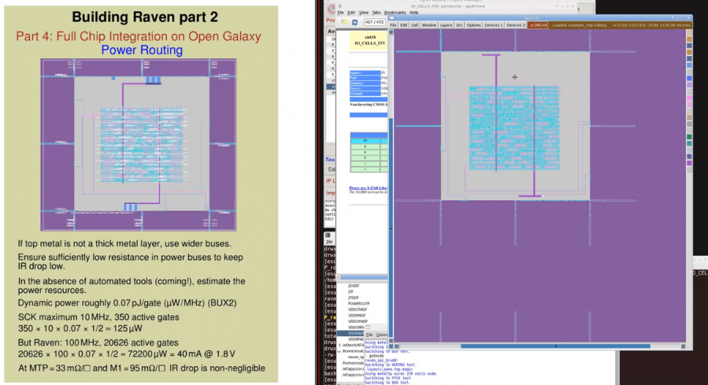
Finally, we have planning of power routing. If you have multiple blocks, make sure you have plenty of channels between blocks, particularly, if they are going to be blocking top level metal. You would be doing most of your power routing on your thick metal layers. If you got thick top-level metal layers, its designed to be your power buses and carry current from chip perimeter to your core. So, use the thick metal where you can. Below is how your power routed raven_spi floorplan would look like

Now these are just few tips to have the best floorplan (in terms of power, performance and area). You are free to come up with your own ways to do the same thing. For few more tips, you might want to check out below course on SoC full chip physical design:
https://www.udemy.com/vsd-soc-design-of-the-picorv32-riscv-micro-processor/
All your ideas will be reviewed by below panel of session chairs (who are all experts in their domains) and you might just get a chance to showcase your innovation to top crowd from VLSI industries:

The reason for this conference is to do out-of-the-box things in field of VLSI, to showcase your versatility and talent to a lot of TOP people, and get their attention, all online.
“This can be your new creative resume”
All the best for your submissions and happy learning


