|
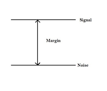
Noise margin is the amount of noise that a CMOS circuit could withstand without compromising the operation of circuit. Noise margin does makes sure that any signal which is logic '1' with finite noise added to it, is still recognised as logic '1' and not logic '0'. It is basically the difference between signal value and the nosie value. Refer to the diagram below.
Consider the following output characteristics of a CMOS inverter. Ideally, When input voltage is logic '0', output voltage is supposed to logic '1'. Hence Vil (V input low) is '0'V and Voh (V output high) is 'Vdd'V.
Vil = 0
Voh = Vdd
Ideally, when input voltage is logic '1', output voltage is supposed to be at logic '0'. Hence, Vih (V input high) is 'Vdd', and Vol (V output low) is '0'V.
Vih = Vdd
Vol = 0
Noise Margins could be defined as follows :
NMl (NOISE MARGIN low) = Vil - Vol = 0 - 0 = 0
NMh (NOISE MARGIN high) = Voh - Vih = Vdd - Vdd = 0
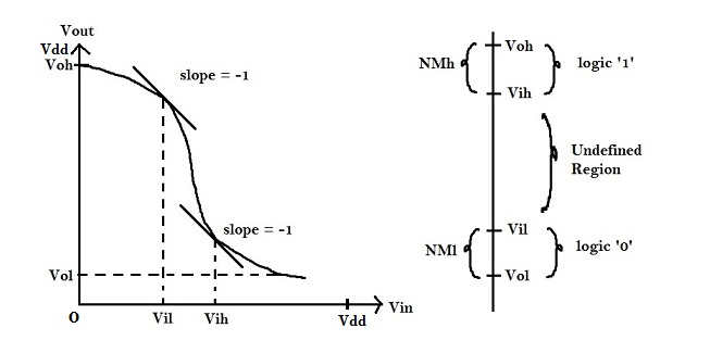
But due to voltage droop and ground bounce, Vih is usually slightly less than Vdd i.e. Vdd', whereas Vil is slightly higher that Vss i.e. Vss'.
Hence Noise margins for a practical circuit is defined as follows :
NMl (NOISE MARGIN low) = Vil - Vol = Vss' - 0 = Vss'
NMh (NOISE MARGIN high) = Voh - Vih = Vdd - Vdd'
Hence, if input voltage (Vin) lies somewhere between Vol and Vil, it would be detected as logic '0', and would result in an output which is acceptable. Similarly, if input voltage (Vin) lies between Vih and Voh, it would be detected as logic '1' and would result in an output which is acceptable.
| 


Comments: