|
In deep sub-micron technology (i.e. <130nm) and below, the lateral capacitance between nets/wires on silicon, becomes much more dominant than the interlayer capacitance. Hence, there is a capacitive coupling between the nets, that can lead to logic failures and degradation of timing in VLSI circuits. Crosstalk is a phenomenon, by which a logic transmitted in vlsi circuit or a net/wire creates undesired effect on the neighbouring circuit or nets/wires, due to capacitive coupling.
Refer to the digram below to get a clear picture on the effect of coupling capacitance on functionality and timing of VLSI circuits.
Crosstalk Noise due to Coupling Capacitance
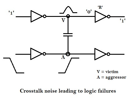
The disturbance at 'A' can potentially cause a disturbance at 'V', because of the mutual coupling capacitance, and if the disturbance at 'V' crosses noise threshold of the receiving gate 'R', then it may change the logic at the output of 'R' i.e., output of 'R', which is supposed to be at logic '1', might switch to logic '0', as it senses a logic '1' at its input, due to the noise induced on its input by the disturbance at 'A'.
Refer to diagram below to understand noise-induced bump characteristics at different noise margin levels.
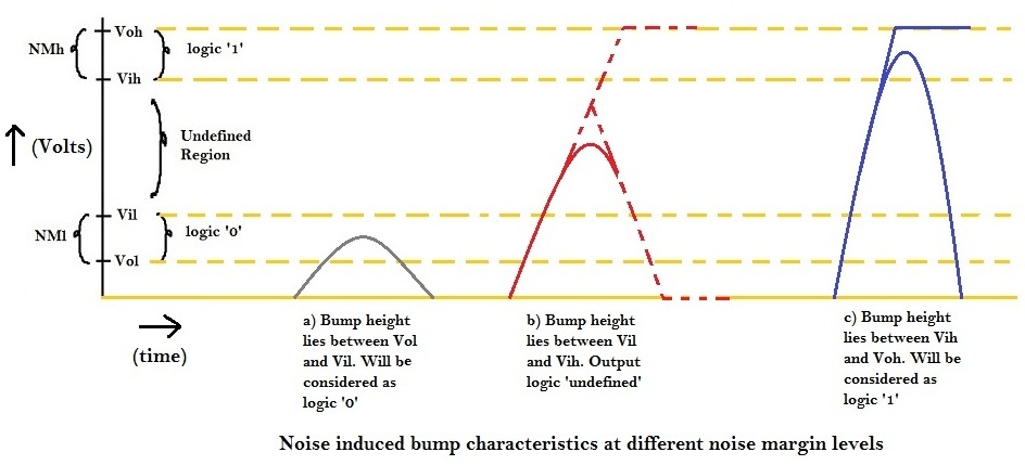
If the bump height at victim 'V' lies between NMl (Noise Margin low), then the logic at victim 'V' will remain at logic '0'.
If the bump height at victim 'V' lies between Vil and Vih, then the logic at victim 'V' is undefined, i.e. it might switch to logic '1' or logic '0'.
If the bump height at victim 'V' lies between NMh (Noise Margin high), then the logic at victim 'V' will switch to logic '1', leading to logic failures.
Timing Degradation due to Coupling Capacitance
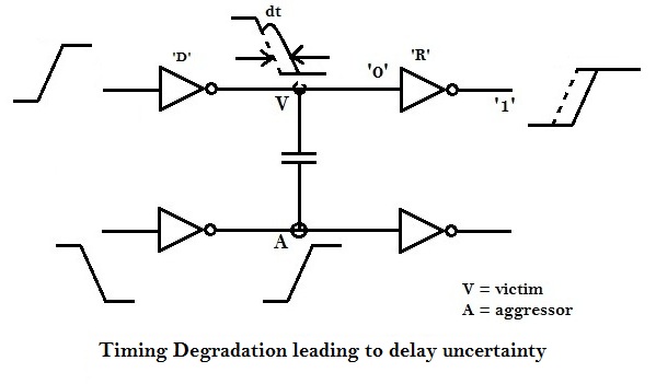
Consider input of driver 'D' switching from logic '0' to logic '1',thus the logic at node 'V' switches from '1' to '0'. Now, if both 'A' and 'V' nodes have signal switching event at the same time interval, then, due to noise induced by signal transition at agressor 'A', a change in the timing instant of the signal transition occurs at 'V', as shown in above figure. Due to this, the propagation delay of the driver 'D' increases by 'dt' amount of time, thus increasing the overall propogation delay of the circuit, which might lead to potential setup violation.
Crosstalk Modelling and AnalysisRefer diagram below to understand the basic model of crosstalk
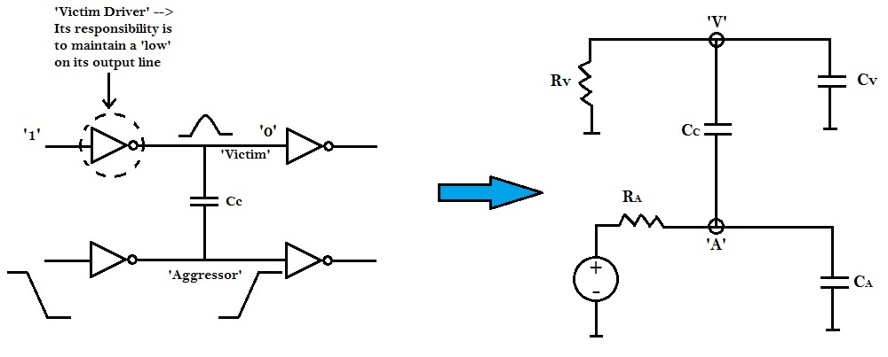
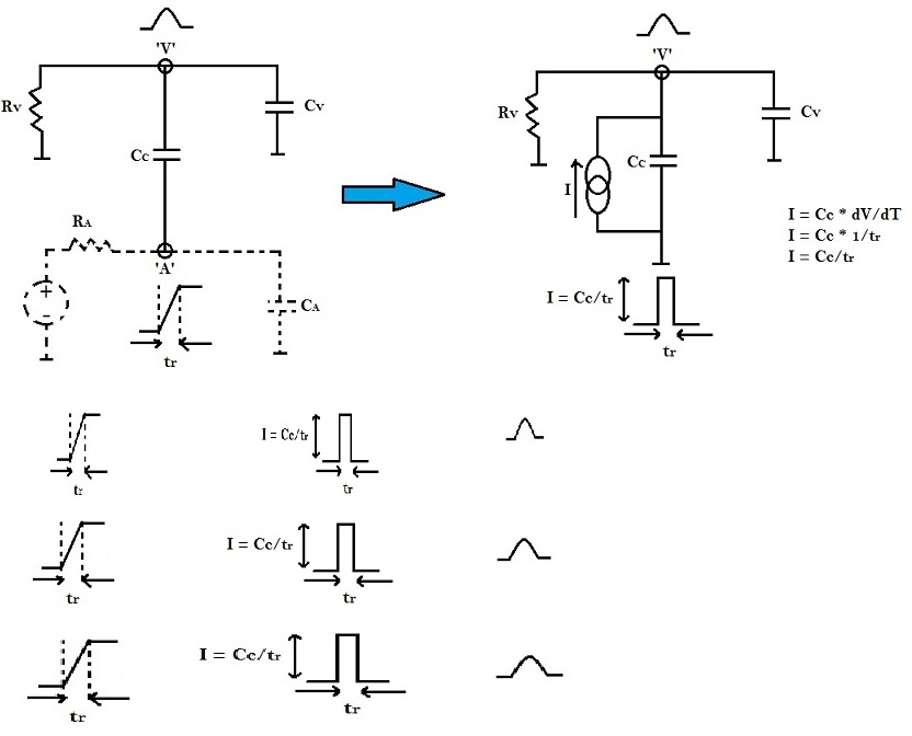
'Victim' and 'aggressors' drivers can be modelled by resistors 'RV' and 'RA', respectively. Whereas 'victim' and 'aggressors' loads can be modelled by capacitors 'CV' and 'CA', respectively. Let the coupling capacitance between them be CC. The above model can be further simplified as shown in figure below.
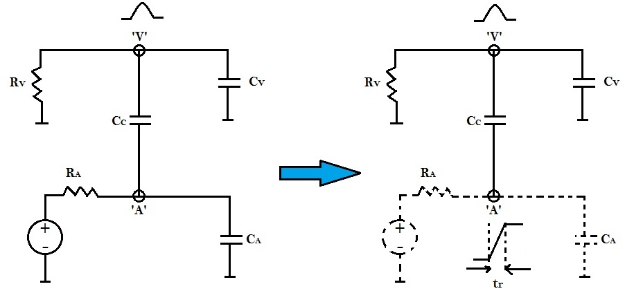
In the above figure, tr is the rise time at the aggressor node 'A', which is related to the gate delay RA as shown in below equation:
tr = RA * ( CC + CA )
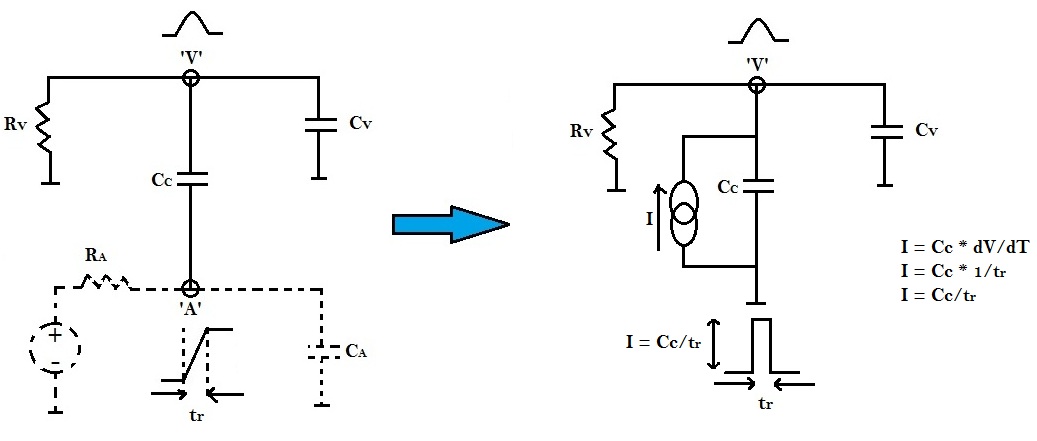
Essentially, the above figure represents a voltage source connected at aggressor node 'A' with a series capacitance 'CC'. By thevinin to norton conversion, this voltage source can be replaced by a current source with parallel capacitance 'CC' as shown below:
We need to find the voltage equation at victim 'V', considering the final value of voltage as Vfinal shown in equation below:
Vfinal = I * R
Vfinal = (CC / tr) * RV
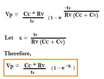
The noise induced bump is nothing but charging-discharging waveform across capacitor as shown below:
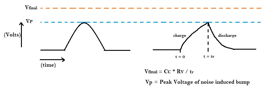
The charging voltage across capacitor can be deduced from the following equation:
Vcharge = Vfinal (1 - e-t/RC)
At t = tr
Vcharge = Vp
R = RV, C = CC + CV
RV * (CC + CV) = Equivalent Time Constant
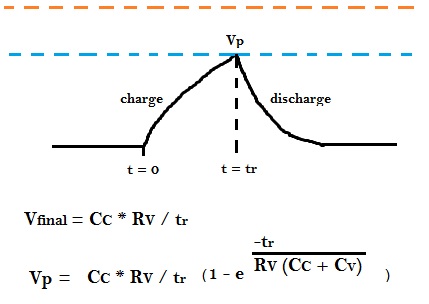
Vp = (CC / tr) * RV (1 - e -tr /(RV *(CC + CV)))
The figure below shows how peak voltage is a function of coupling capacitance CC, Victime drive strength RV and rise time on aggressor line.
The higher Vp is, there are more chances that it would exceed noise margin. But, that is not the only thing.
Consider a case, where the pulse height Vp is high (1V), with small pulse width (e.g. 1ps) as opposed to another scenario, where the pulse height is low (e.g. 0.3V) and pulse width is large (e.g. 100ps). This can be illustrated in the diagram below.
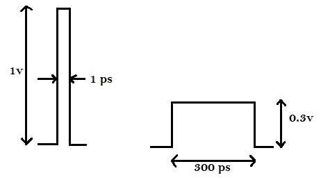
If the receiving gate's RC delay is not in sync with the incoming pulse, it may not even recognise the incoming pulse (1V, 1ps). Therefore, even if the peak of the pulse is substantial, but pulse is narrower, its possible that the receiving gate doesnot identify the existence of that pulse and it gets filtered out.
Therefore, we have 2 things to control
1) Peak Voltage (Vp)
If x is very very small i.e. Rv(CC + CV) is large compared to tr, then e-x ~ (1 - X)
Therefore, Vp can be deduced as shown below:
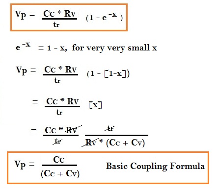
Hence, the first solution to reduce crosstalk noise, is to increase the Resistance of Victim driver (RV).i.e. downsize the victim driver, so that, the high resistance of the victim driver restricts the supply of current and charging of victim net capacitance during the rise time (tr) of aggressor signal, which would in turn reduce the bump height.
The second solution to reduce crosstalk noise, is to increase the Capacitance of Victim load (CV).i.e. upsize the victim load, thus the resistance will reduce, which will in turn help the victim net to maintain a strong static voltage.
2) Pulse Width
Pulse width, depends upon the agrgressor net transition. The steep the transition is, on aggressor, the shorter will be the pulse width. This can be illustrated as shown in below diagram.
Hence, the third solution to reduce crosstalk noise, is to maintain sharp transitions on aggressor.
Another method to reduce crosstalk noise is to introduce shields in between victim and aggressor. Back to Introduction to Physical Design Forum
|