Propagation Delay of CMOS inverter
The propogation delay of a logic gate e.g. inverter is the difference in time (caluclated at 50% of input-output transition), when output switches, after application of input.

In the above figure, there are 4 timing parameters. Rise time (tr) is the time, during tansition, when output switches from 10% to 90% of the maximum value. Fall time (tf) is the time, during transition, when output switches from 90% to 10% of the maximum value. Many designs could also prefer 30% to 70% for rise time and 70% to 30% for fall time. It could vary upto different designs.
The propagation delay high to low (tpHL) is the delay when output switches from high-to-low, after input switches from low-to-high. The delay is usually calculated at 50% point of input-output switching, as shown in above figure.
Now, in order to find the propagation delay, we need a model that matches the delay of inverter. As we have seen above, the switching behavior of CMOS inverter could be modelled as a resistance Ron with a capacitor CL, a simple first order analysis of RC network will help us to model the propagation delay.
First order RC network
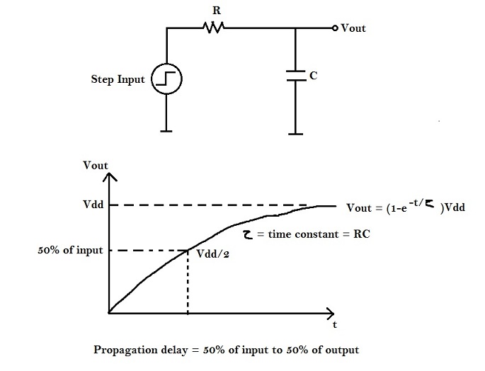
Consider the following RC network to which we apply a step input.

Our aim is to find 't' at Vdd / 2.
Vout = (1-e-t/τ) Vdd, where τ = RC = time constant.
Substituting 'Vout' equal to Vdd/2, and 't' equal to 'tp' in above equation, we get the following :
Vdd/2 = (1-e-tp/τ) Vdd
Therefore, tp = ln(2) τ = 0.69τ
Hence, tp = 0.69RC
Hence, a CMOS inverter can be modelled as an RC network, where
R = Average 'ON' resistance of transistor
C = Output Capacitance
Engineering Change Order (ECO) is the process of modifying the PNR netlist in order to meet timing (i.e. setup, hold, transition and max_capacitance) requirements. For eg. if there's a setup violation in the design, it implies that a combinational path has large delay than required. In this case, you need to reduce the delay by upsizing cell, which reduces resistance, in turn, reduces RC delay of the path.
Following sections explains the concepts needed to modify delay of a particular logic cell. Inverter has been considered as an example.
Below figure shows that the output capacitance (CL) of an inverter is constant, and the input slew is varying.
From the above figure, if input transition is high, it helps or reduces the propagation delay. But, on the other hand, it disturbs signal integrity. This implies, the circuit should not be over-designed i.e. if a circuit could run at an input transition of 50 ps, it should not be designed to run at 20 ps.
"Delay reduces with increase in input transition and constant load capacitance"
Consider, another scenario, where input transition is constant, whereas, output capacitance is varying. This is captured in the following diagram
As shown in the above figure, as output capacitance increases, the total time required to charge this capacitance increases, hence RC delay increases. This could be helpful in fixing hold violations where delay needs to be increased to meet hold margin.
"Delay increases with increase in output capacitance and constant input transition"
The above two examples shows that the delay of cell directly depends on input transition and output capaciance.
Another technique to modify the delay of cell is to 'upsize' or 'downsize' a cell i.e. varying the drive strength ('ON' resistance) of the cell. This is captured in the figure below
High drive strength cell indicates a cell having low 'ON' resistance. Due to low resistance, the time required to charge the output capacitance will be low, i.e. RC delay reduces. This technique is useful to fix setup violation where the delay needs to reduced. The inverse (i.e. high 'ON' resistance) is useful for fixing hold violation, where the delay needs to increased.
"Delay varies by varying drive-strength (ON resistance) of the logic cell"
Another intelligent method, but a leaky one, to reduce the delay of cell is to swap high threshold voltage (Vt) cell with low Vt cell. Refer to the below diagram
The characteristics of NMOS (or PMOS) device is such that, the 'ON' resistance is inversely proportional to (Vgs - Vt). But, the direct effect is that low Vt cells are often more leaky i.e. leakage power increases.
"Delay can be reduced by using low Vt cells, but the cost paid is high leakage power"
|