|
Static Timing Analysis (STA) is one of the techniques to verify design in terms of timing. This kind of analysis doesnot depend on any data or logic inputs, applied at the input pins. The input to an STA tool is the routed netlist, clock definitions (or clock frequency) and external environment definitions. The STA will validate whether the design could operate at the rated clock frequency, without any timing violations. Some of the basic timing violations are setup violation and hold violation
Consider the following Mealy Machine diagram to understand setup and hold timing checks

Above figure shows a basic description of a system in form of a Mealy Machine. Consider a flip-flop 'X' which generates data 'Din and it arrives as inputs to Mealy Machine after some delay q'(current state). Mealy Machine generates an output 'Dout', at q (next state). The receiver 'Y' receives 'Dout' after some delay.
The common thing between the flip-flops X, Y and Z is the 'clock'. Same 'clock' is used to control all transfer of data between flip-flops. On the same clock edge, there would be some change at the output of X, there would be a change in the output of 'Z' and the change would propagate to q and 'Dout' after some delay. 'Dout', after some delay would propagate all the way to 'Y'. For correct operation, this change in 'Dout' should be captured at next clock edge by 'Y'.
Hence, correctness of the system can be judged by tracing each Sender - Receiver pair. In the above example, Sender is 'X' whereas Receivers are 'Y' and 'Z'.
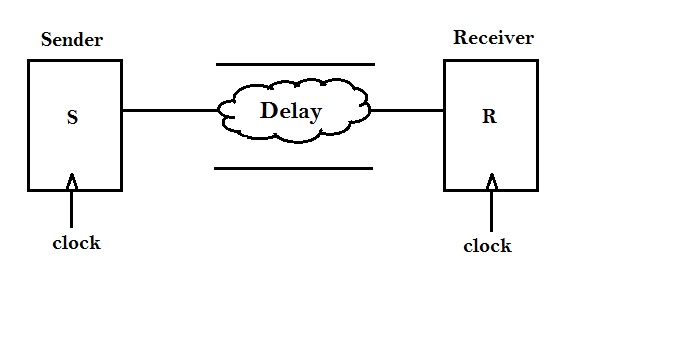
Above figure shows a Sender-Receiver pair. Assume, identical clock goes to both and there's some delay between Sender and Receiver. This delay will not be fixed as the effective load capacitance seen by each gate in the design is different. Other factors that affect the delay of a gate such as input transition, threshold voltage, drive strength, etc.
Let us study the following example of a NAND gate to understand how the delay varies within a gate.
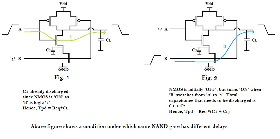
Assume that output was at logic '1', which means either 'A' or 'B' was at logic '0' and other at logic '1'.
Consider 'B' was at logic '1', and 'A' at logic '0'. Output will switch from logic '1' to logic '0', when 'A' switches from logic '0' to logic '1' (Fig. 1). Let us consider this as Delay I.
Consider 'A' was at logic '1', and 'B' at logic '0'. Output will switch from logic '1' to logic '0', when 'B' switches from logic '0' to logic '1' (Fig. 2). Let us consider this as Delay II.
Now the question is, "Is Delay I and Delay II same or different? If different, which delay path is faster (I or II)? Why?"
In Fig. 1, as 'B' is already at logic '1', the NMOS, to which 'B' is connected is already 'ON' and hence the capacitor C1 is already discharged. So, when 'A' switches from logic '0' to logic '1', only capacitor CL has to be discharged through the pull-down NMOS network.
Whereas, in second case (Fig. 2), the NMOS to which 'B' is connected is 'OFF', since 'B' was at logic '0'. So, now, when 'B' switches from logic '0' to logic '1', capacitors C1 and CL, both has to be discharged through the pull-down NMOS network, which takes more time compared to Delay I.
Hence Delay I and Delay II are different, where Delay I is less than Delay II.
The above example illustrates for 2-input NAND gate, it has two timing paths.More complex logic gates will have even more timing paths, e.g. 10 input MUX. Thus, the delay between Sender and Receiver is not constant, but will have range of values, as shown below.
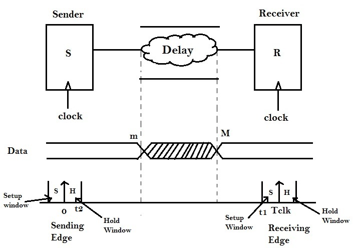
Therefore, the delay ranges from m ≤ delay ≤ M.
Where m = minimum propagation delay of combinational logic
and M = Maximum propagation delay of combinational logic
There is a requirement from the receiver (basically, a flip-flop), that, if it has to sample data at Tclk, the data should be available and stable before or at finite time (say 't1'), before clock edge Tclk arrives. Therefore, (Tclk - t1) is the setup time or setup margin or setup window (S) for the data to arrive to the receiver.
On the other hand, there's a requirement from Sender (again, a flip-flop), that if data has to change after sending clk edge, that change should happen atleast after a finite time (say 't2'), after clock edge arrives. If this change in data happens before 't2', it might corrupt the data, which the flip-flop has already sampled. This finite time period 't2' is called as Hold time or Hold margin or Hold window (H).
The finite time periods 't1' and 't2' are the internal delays of a flip-flop
The data is not expected to change between hold time 'H' to 'm' and 'M' to (Tclk - Setup time 'S'). Data changes somewhere between 'm' and 'M', and becomes stable after that.
Therefore, we have got certain defining equations for setup and hold time, and they are as follows :
m > H i.e. Minimum propagation delay of the combinational logic should be greater than Hold Margin
If m < H , it results into timing violation, called as Hold violation. This means, that the combinational logic delay is very less and hence data change is very fast. To satisfy the 'hold' requirement, the combinational logic delay should be increased.
M < Tclk - S i.e. Maximum propagation delay of the combinational logic should be less than Clock period (Tclk) minus the Seup Margin
If M > Tclk - S , it results into timing violation, called as Setup violation. This means, that the combinational logic delay is very large and hence data change is very slow. To satisfy the 'setup' requirement, the combinational logic delay should be decreased.
The process of fixing timing violation, and implement the fixes back to the PNR netlist, is referrred to as Engineering Change order (ECO) .
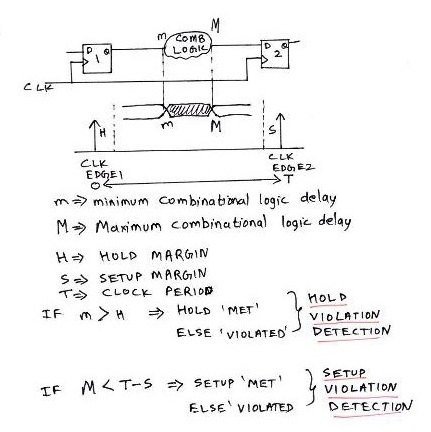
Above figure summarizes the concept of setup and hold time for an ideal clock (i.e. both sender and receiver are clocked at the same time).
But, on a chip, this is usually not the case. Due to wire RC's, the clock might not reach the sender or receiver at the same time. It is possible, that clock for sender reaches at Δ1 and clock for receiver reaches at Δ2. This clock network delay could captured in the following diagram.
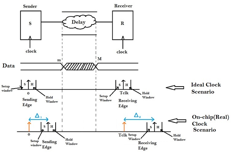
In the above figure, clock to sender reaches at Δ1 and not at '0', whereas, clock to receiver reaches at (Tclk + Δ2 ) and not at Tclk. The modulus difference between Δ1 and Δ2 (|Δ1 - Δ2|) is referred to as skew.
Now, the defining equations for setup and hold time will change, and they are as follows :
m > H + Δ1 i.e. Minimum propagation delay of the combinational logic should be greater than Hold Margin + the clock network delay for sender
M < (Tclk - S) + Δ2 i.e. Maximum propagation delay of the combinational logic should be less than Clock period (Tclk minus the Setup Margin ) + clock network delay for receiver i.e. Δ2
Now, consider the following scenario, where there is only one sender, and multiple (say '10') receivers.
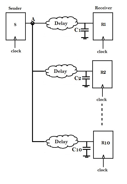
In the above scenario, node 'A' is connected to '10' Receivers, i.e. the load on node 'A' has increased '10x' times compared to previous examples. So now, the time required for node 'A' to charge all the '10' input capacitances of the receiver, will increase, and the waveform at 'A', will look like as shown in figure below.

Every system has got a margin for 'transition' or 'slew' (say tslew) and 'max capacitance' (say Cmargin). Hence, if the transition (or slew) on node 'A' exceeds tslew, it would result into timing violation, usually called as 'transition' violation.
Similarly, if the capacitance on node 'A' exceeds Cmargin, it would result into violation, usually called as 'max_capacitance' violation.
The best way to fix max_capacitance and transition violation, is to either increase the drive strength of the Sender or buffer tree insertion
Following figure summarises transition and max_capacitance requirement and violations.
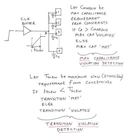
Above figure shows an example of transition and max_capacitance violation on the output pin of clock buffer, which is conected to the 'clk' pin of 'n' receivers. Back to Introduction to Industrial Physical Design Flow
Back to Crosstalk
|
Comments: